yosys4gal: a Yosys Synthesis flow for GAL chips
- Description
- Bringing modern synthesis to 30-year old technology with Yosys and Rust.
- Date
- tags
- rust
- vlsi
GAL/PALs are ancient chips designed to implement custom logic as a precursor to CPLDs and FPGAs. They can implement any combinational logic using a Sum-of-Products architecture and a grid of wires with certain wires being connected at different coordinates:

Later GALs added more features like feedback, tri-state pins, and D Flip-Flops for sequential logic.
They're pretty neat, except for the part where they're a nightmare to program. Instead of using Verilog or other HDLs, which didn't exist at the time, designers would manually specify the minterms of each output:
gal16v8
CombTest

Clock I0    I1    I2    I3    I4    I5    NC    NC   GND
/OE   O0    O1    O2    O3    O4    I6    NC    NC   VCC

O0 = I0 * I1

O1 = I2 + I3 + I6

O2 = I4 * /I5 + /I4 * I5

O3 = I0 * I1 * I2 * I3 * I4 * I5

/O4 = I0 + I1 + I2 + I3 + I4 + I5

DESCRIPTION

Simple test of combinatorial logic.
I don't want to deal with this. It's annoying to think about. What if we could create our own Verilog flow for GAL chips? Then we could take advantage of the simulation and synthesis capabilities, which would make these chips a bit more useful.
The idea
We use Yosys to synthesize Verilog, and do technology-mapping onto a set of
primitive blocks that are then mapped by a custom tool. Our custom tool takes
the place of nextpnr in the standard open-source gateware flow. It will be
responsible for mapping the techmap onto actual positions based on a pin
constraints file.
There's two components - Yosys technology mapping, and writing a "place-and-route" tool. We'll start with Yosys.
Yosys Technology Mapping
This process is cursed and low level, but it works a little like this:
- Yosys takes a generic synthesis pass at a netlist, which simplifies the design without looking at any physical implementation
- We use Berkeley's
abcto convert the logic into sum-of-product form. - The simplified design is then mapped into Verilog-based "blocks", which could be things like AND gates, or complex blocks like a LUT. This process turns generic blocks like an adder into a set of gates.
- certain sequences of gates are then grouped and unified in the "extract" pass. Extraction would convert an operation like
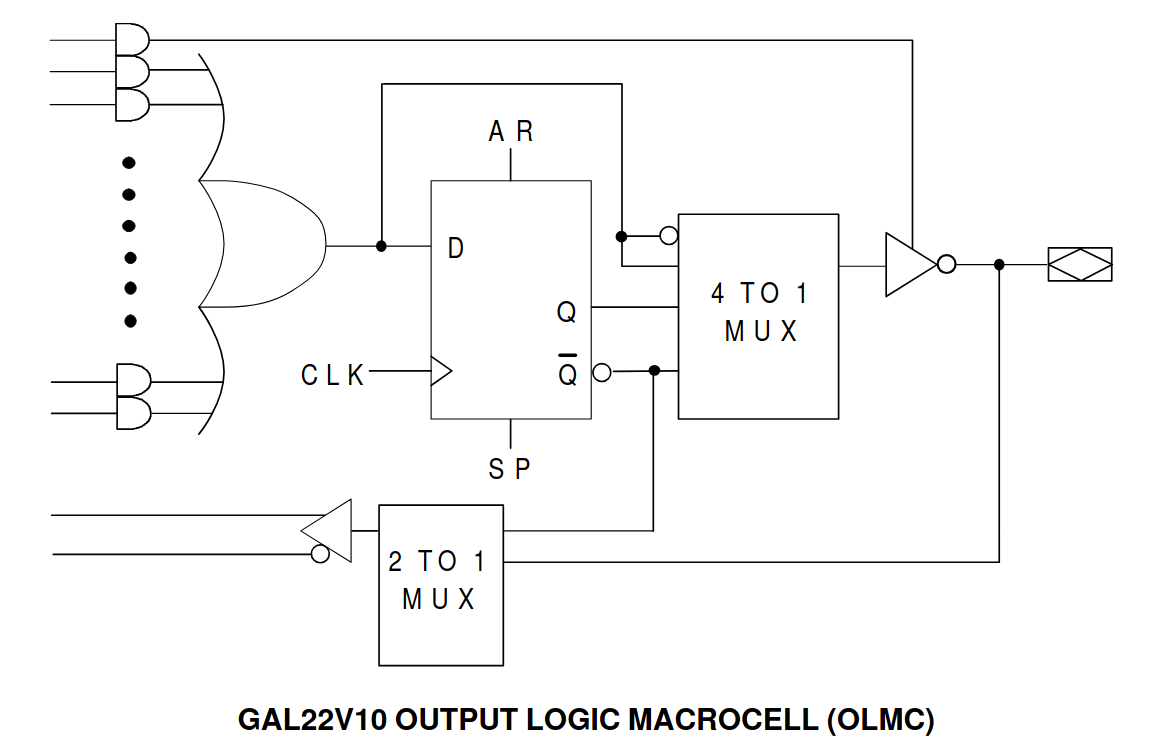
mul -> addinto a singlemul_addblock. - we do some other passes to make the design more homogeneous. Each OLMC has a unique "GAL_SOP" term and each SOP only takes inputs
from OLMCs or
GAL_INPUTblocks to make it easier to identify.
The Verilog model
A history lesson
During the semiconductor revolution, a dilemma appeared: Designing new integrated circuits required a lot of time and effort to create the mask, and iteration expensive. Due to limited tooling, ICs could not be complex designs. Techniques and tools to do tasks like optimization or place-and-route did not exist or were primitive. And what if you wanted a low-volume design? Programmable Logic Arrays (PLAs) were an early approach to these problems. The idea was simple: create a flexible logic architecture to allow for engineers to prototype new digital designs. These worked by using matrices of wires in a Sum-of-Products architecture. Inputs would be fed with their normal and inverted forms to a bank of AND gates, which would select inputs using a fuse tie on the die and create product terms. The outputs of the AND gates would then be fed into OR gates, which would create the sum term for the whole output.
This design was popular, since it allowed for less-certain aspects of the chip to be moved to a later design process. Eventually, hardware people got jealous of the fast (for the time) compile-eval loops in software, and so some smart engineers created PAL (Programmable Array Logic).PAL is similar to PLA logic, but the fuses are programmed using a simple programmer rather than a complex die process. This means that a developer with a pile of chips can program one, test it, make some adjustments, and then program the next. Later versions would solve the whole one-time-programmable aspect using UV-erasable EEPROM.
Demands would increase further and flip-flops would be added, as well as feedback capability. This allows for implementation of functions that would otherwise be too large to fit in a single logic term, since you can chain "rows" of the output blocks. This culminated in the GAL22V10, which is an electronically-erasable, 22-pin programmable logic block, which had up to 10 outputs that are registered and used for feedback. These outputs are also capable of tri-state (input or output switchable during operation) to give greater flexibility.
Back To Today: GALs in the 21st Century
These days, modern FPGA technology can be yours for a couple of bucks. Open-source toolchains allow fast, easy development, and the glut of Verilog resources online makes it easier than ever to enter the world of hardware design. But there are times when GALs might still be useful. For one, they start up instantly. Some FPGAs have a fast one-time-programmable internal ROM, but this loses the "field-programmable" aspect which makes FPGAs desirable. In most cases the bitstream loads from an external SPI flash. This can take up to a few seconds, which may not be acceptable if the logic is critical. Another important factor is the chip packaging. Most FPGAs are BGA packages, with some offering QFN or even a few QFP variants, but none are available in any DIP form factor, at least without a small board in between. The ATF22V10 (which is a clone/successor of the GAL22V10) is available in DIP, SSOP, and even PLCC if that's your jam. The package options make GALs perfect for breadboard applications. You could use it like an 8-in-1 74-series logic chip, changing the function depending on what you need. Additionally, GALs operate at 5 volts is useful when interfacing with older systems and removes the need for a level shifter.
In practice, this isn't all great. Programming GALs is an exercise in frustration. Take a look at a basic combinatorial assembly file:
gal16v8
CombTest

Clock I0    I1    I2    I3    I4    I5    NC    NC   GND
/OE   O0    O1    O2    O3    O4    I6    NC    NC   VCC

O0 = I0 * I1

O1 = I2 + I3 + I6

O2 = I4 * /I5 + /I4 * I5

O3 = I0 * I1 * I2 * I3 * I4 * I5

/O4 = I0 + I1 + I2 + I3 + I4 + I5

DESCRIPTION

Simple test of combinatorial logic.
In the contrived example the behavior is pretty clear, but it's not exactly a stellar format for writing complex logic. Plus, there's no way to integrate or test this in a larger system (we'll get back to this). Compared to the Verilog flow, with simulation, testbenches, and synthesis, the raw assembly is stuck in the 80s and requires manual logic simplification.
Verilog compilers for GALs did exist, but they ran on old-as-dirt systems, didn't have any significant optimization capabilities, and were almost always proprietary. What if we could make our own open-source Verilog flow for GAL chips? Then we could write test benches in Verilog, map complex designs onto the chip, and even integrate our designs with FPGAs later down the line.
The idea
GAL assembly appears occasionally when working with older systems, especially in a retro emulation context.
Is this useful?
Not particularly.
Well, there is a niche use case. These parts are 5-volt tolerant, and come in DIP packages. If you needed some basic glue logic when working on an older 5 volt system, you might want to have a few of these and a programmer instead of a collection of 74-series logic. These chips can emulate any 74-series chip, and can reduce a multi-chip design to a single chip. The DIP form factor makes it much easier to breadboard, and the chips have zero start up delay.
In that narrow use case, yosys4gal is rather crucial. You no longer need
WinCUPL or any old software, instead using Verilog + Yosys. Your designs are
automatically optimized, which makes it easier to fit more complex logic. And
since it's Verilog, you can integrate it into a larger simulation or move it to
an FPGA later if you desire.